How to glue SMD resistors onto the board. SMD components and recommendations for soldering printed circuit boards. Most common mistakes
Gone are the days of introductory radio parts, with the help of which a radio amateur repaired tube televisions and old radios. SMD elements, much more compact and high-tech, have become a fixture in our lives. What is this SMD component? To put it in the words of those who began assembling and repairing devices in the days of transistor radios, these are “small dark things with inscriptions that are completely incomprehensible.” But seriously, if we decipher the term “SMD-component” and translate it into Russian, we get “surface-mounted”.
Tracking resistance characterizes the strength of the surface insulation insulating materials, in particular, under the influence of moisture and impurities. It defines the maximum leakage current that can be established in a particular test arrangement under standardized test conditions.
A short circuit is a connection between two points that may not exist according to the diagram. Short circuits are compounds that, for example, tin threads, poor etching or mechanical damage insulating layer between layers.
What does this mean? Surface mounting (planar mounting) is a manufacturing method in which parts are placed on a printed circuit board on one side with contact tracks. No drilling is required to locate radio components. This method is the most common these days and is considered the most optimal. On an industrial scale, printed circuit boards based on SMD components with high speed“stamped” by robots. A person can only do what a machine cannot yet do. It is necessary to understand why SMD components are so good and whether they have any disadvantages.
For each network, a reference point is defined as a primary reference point. The isolation between all networks is then measured. When PCB 3 has nets, mesh 1 is measured over mesh 2, mesh 1 over mesh 3, and mesh 2 over mesh 3. If additional nets are present, the number of measurements is as follows.
Solder resistance during production process
In the history of integrated microelectronics, various families of circuits have been developed that differ in terms of the functional principles used and their associated characteristics. With new design and manufacturing technologies, users now have the ability to create and use custom ASICs as well as standard circuits.
Advantages of installation
Example of a board with SMD components
Naturally, with the incredibly small sizes that SMD elements have, the finished printed circuit boards are very compact, from which we can conclude that the finished device based on such a platform will be very big size. When printing, less fiberglass and ferric chloride are required, which significantly increases savings. In addition, the manufacturing time required is significantly less, since there is no need to drill holes for the legs of various elements.
Most single and double sided platinum printed circuit boards produced by photochemical means. Current order of production steps. Drilling through contact photoresist Exposure lamination Development of etching Washing Drying. Subsequent processing steps then follow.
After double-sided PCBs with a copper layer on both sides of the PCB, several thinner PCBs began to appear with so-called multilayer PCBs, which can now have up to 48 layers, in some cases more. For example, from four to eight layers in computers and up to twelve layers in mobile phones. The connections between layers are made with through holes.
For the same reason, such boards are easier to repair and replace radio components. It is even possible to manufacture a printed circuit board by installing SMD elements on both sides, which could not even be imagined before. And, naturally, the price of chip components is much lower.
Of course, in addition to advantages and disadvantages (what would be without them). Platforms based on SMD components do not tolerate kinks or even minor mechanical impacts (such as shocks). From them, as well as from overheating during the soldering process, microcracks can form on resistors and capacitors. Such problems do not make themselves felt immediately, but appear during the work process.
In many cases, the use of multi-layer PCBs is also necessary at lower packaging densities, to ensure low-induction power to all components. Prepreg refers to a semi-finished product consisting of continuous fibers and an uncured thermoset plastic matrix, a. V lightweight design. Continuous fibers may be present as a pure unidirectional layer, like fabric or fabric.
What is surface mounting?
Prepreg is supplied in the form of a web wound on rolls. Prepregs are machine processed and hence are mainly used in automated processes. They give smooth and high quality. Structured in layers separated by function. The structure of one or more layers of copper.
And, of course, those who encounter chips for the first time do not understand how they can be distinguished. Which one is a resistor and which one is a capacitor or transistor, or what sizes can SMD components have? All this needs to be sorted out.
Types of SMD element housings
All such elements can be divided into groups based on the number of pins on the body. There can be two, three, four-five, six-eight. And the last group is more than eight. But there are chips without visible pins. Then there will be either contacts or solder in the form of small bumps on the case. SMD components can also differ in size (for example, height).
Housings and sizes
Before mass production, it is often recommended to test the circuit without risking high cost creating photo masks. The following options are available. Manufacturers offer the production of individual products and small series in the "pool", a few hours individual parts drilled into a large plate, coated, exposed, etched and then crushed.
Mesh hole boards have holes or solders in the mesh which is commonly used for electronic components, i.e. 2.54 mm, which corresponds to 0.1 inches or half of them. They can be separated, if required, by the tool using a conductor track recording. In the milling technique, the dividing lines between the surfaces of the conductor are made using a milling head. All copper remains except dividing lines. Surface and photolithographic steps are omitted.

Types of SMD elements
In general, markings are affixed only to larger chips, and even then they are very difficult to see. In other cases, it is impossible to figure out what kind of element is in front of your eyes without a diagram. SMD components come in different sizes. It all depends on their performance. More often than larger size chip, the higher its value.
Characteristics of relief boards
The design is printed onto suitable paper or specially made heat resistant foil with a laser printer and then "ironed" onto the PCB using an iron or laminator. The toner becomes a light liquid, like in a printer's fuser unit, and bonds to the copper of the circuit board. The paper is then cleaned again with water - the toner remains on the copper. An etching process then follows, leaving the remaining areas covered with toner. The toner can then be removed by dilution. In this method, tolerances can occur as the paper is transported in the printer and as the paper is stretched and contracted by heat.
SMD chokes
Such chokes can be found in different types cases, but their standard sizes will be similar. This is done to facilitate automatic installation. Yes and to a simple radio amateur it's easier to figure it out that way. Any inductor or inductor is called a "winding product". Perhaps, for older equipment, such a circuit element could be wound with your own hands, but with an SMD component such a number will not work. Moreover, the chips are equipped with magnetic shielding, they are compact and have a wide operating temperature range.
The feeder can be safely placed on the machine, slipping is not possible. This allows the feed to be optimally adapted to the equipped components. Vibration is started automatically by removing a component and ends automatically after a set duration. This ensures that sufficient components are always available.
This feeder is pneumatically controlled, the components are covered during feeding. Possible width - 10 poles. In particular, when creating large-format matrix displays, it is advisable to use such a feeder. For the production of foil inserts, there are feeders for feeding quick-action discs. Feeders can promote everything standard sizes instant discs. Customized solutions can also be easily implemented.
You can select a similar chip from the catalog based on the required standard size. This parameter is set using 4 digits (for example, 0805), where 08 is the length of the chip, and 05 is its width in inches. Therefore, the size of the SMD coil will be 0.08 × 0.05 inches.
SMD diodes and SMD transistors

For prototype assembly, it is preferable to use belt section feeders. With this system, up to ten 8 mm belts or correspondingly smaller belts can be fed simultaneously. Therefore, purchasing large rolls is not required. As a result, the placement space can be modified to suit individual project requirements.
It is mechanically linked to the machine for stable removal, can be integrated into the user interface and can be retrofitted with existing machines. Its axis controller ensures gentle movement of high-quality components, and the tray traction does not require indexing in any order.
SMD diodes are either cylindrical or rectangular. The distribution of standard sizes is the same as for chokes.
The power of SMD transistors can be low, medium and high, the difference in the packages depends precisely on this parameter. Of these, two groups are distinguished: SOT and DPAK. Interestingly, one package can contain several components, for example, a diode assembly.
Because we have all the development, design and manufacturing in house, we also solve problems that you can't use standard feed units. If you have any questions, please contact our headquarters in Kastle-Utzenhofen. Most of them look worse than they are. For whom this is too little: with a good magnifying glass you will be amazed at how great it really is.
Resistors, capacitors, inductors and everything with two connections
If you use a fine pencil to make two strokes as close together as possible without touching, you'll get half a millimeter and less space between them pretty quickly. For all components that need to be mounted on a two-pin PCB, you can basically do the same thing: tilt the pad, hold the component with tweezers, and melt the tin on the pad with a soldering iron. Then place the component in position and remove the soldering iron. It sounds simple, but it is true.
In general, SMD parts themselves are of great interest not only for professional radio amateurs, but also for beginners. After all, if you look at it, soldering such printed circuit boards is not an easy task. It’s all the more pleasant to learn to understand all the markings of chips and learn, strictly following the diagram, to replace burnt-out SMD parts with new ones or dismantled from another platform. In addition, the level of proficiency with a soldering iron will increase many times over, because when working with chips it is necessary to take into account many nuances and exercise extreme caution.
Only if the components become so small that as soon as one gets even close to the soldering machine, all the tin melts on any contact, should you also hold the component with a second pad. For components in this category, special tweezers with flattened tips are available that allow you to firmly hold the component in position. The soldering tip doesn't have to be particularly good for this kind of work, a large thumb width is sufficient.
Two capacitors must be soldered onto these pads. To do this, the pads are first canned. 

The first capacitor is then soldered to the tinned pad, as is the second capacitor. 
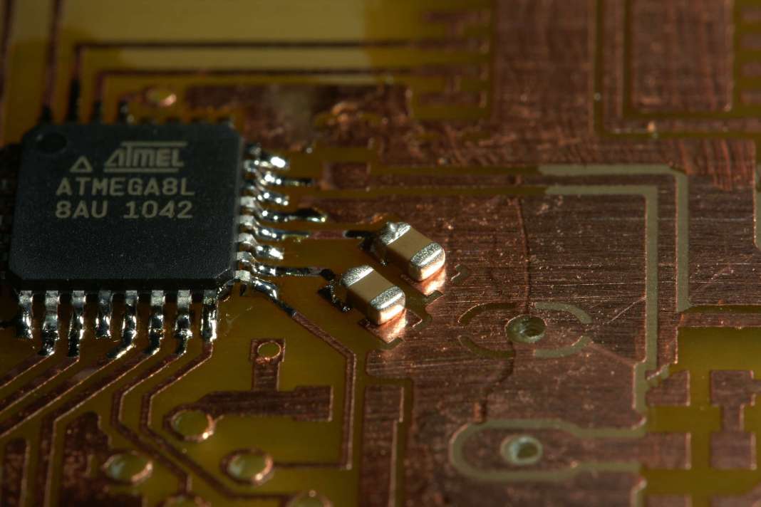
Now only the contact pins need to be soldered on the pads.
Nuances when soldering chips
It is best to solder SMD components using a special station, the temperature of which is stabilized. But in her absence, naturally, only the soldering iron remains. It must be powered through a rheostat, since the heating temperature of the tip of such devices is from 350 to 400 degrees, which is unacceptable for chip components and can damage them. The required level is from 240 to 280 degrees.


But there are several ways, depending on how thin your engine is on the road and what equipment is available. The easiest way is to cover the entire chip with tin and then remove the excess tin again. Then you can rest on all the pins with thick caterpillar. When this is done, either the iron desoldering, tin aspirator or desoldering will be removed. This removes the tin so that only the pins and their spacers remain. Also commonly used here regular soldering iron, at least for example.
It is impossible not only to overheat SMD elements, but also to overexpose the soldering iron tip to the contacts. It is better to use solders that do not contain lead, since they are refractory and it is problematic to work with them at the recommended temperature.

Soldering a printed circuit board
However, the process can damage sensitive chips because the chip typically takes longer to heat up than recommended. Often, with a clean soldering tip, twice the bridge size is enough to melt, since there are tin sticks on the tip. Proper fluxes also help here. To avoid bridges, the tip should only be supplied with tin. A thin solder wire is very important, otherwise the tip always flaps like a thick pearl tin, and then it will never work.
Assembly and installation of elements on printed circuit boards


If the gaskets are accessible from the outside, you can proceed as usual. However, due to the small contact area, soldering takes longer. This is where thin soldering wire again pays, as you can apply a small tip of solder to the tip to optimize the contact surface. But in fact only confuse, not coat with tin! then install the component and, depending on the size of the pads on the PCB, use a soldering iron or hot air soldering iron.
In soldering areas, mandatory tinning of the tracks is required. It is better to hold the SMD element with tweezers, and the duration of contact of the soldering iron tip to the chip leg should not exceed one and a half to two seconds. You need to work even more carefully with microcircuits.
First, the outer legs are soldered (you must first accurately align all the pins with the contacts), and then all the rest. If solder gets on two legs and the leads stick together, you can use a sharpened match. It needs to be laid between the contacts and touched with a soldering iron to one of them.
Common mistakes when soldering
Often, when soldering SMD components, 3 main mistakes are made. But they are not critical and can be corrected.
- Touch the contact with the very end of the tip for fear of overheating. Under this condition, the temperature will be insufficient, so you need to try to solder in such a way that there is a maximum contact surface, only in this case you will get a high-quality mounted board.
- Using too little solder and taking too long to solder. In this case, part of the flux evaporates. The solder does not form a sufficient protective layer, and as a result oxidation occurs. Perfect option– simultaneous contact with the contact of both the soldering iron and the solder.
- Very early removal of the soldering iron from the contact. Although you should act carefully and not overheat the chips, the warm-up time should still be sufficient for high-quality soldering.
For training, it makes sense to take any unnecessary printed circuit board and learn how to solder.
Soldering the chip board
So, without exerting excessive effort, you can start soldering printed circuit boards. The holes that are present on it do an excellent job of fixing the elements. A little experience, of course, won’t hurt here, because that’s what the training was done on an unnecessary platform. Initially, in addition to the tip, solder is also supplied to the contacts, and this must be done in such a way that there is uniform heating of both the terminal and the platform (point of contact).
Solder should be removed after the contact point is completely and evenly covered with it. Next, you need to remove the soldering iron, and then wait until the tin cools down. And only after this can the installation of SMD components be carried out. Afterwards, you must check the quality of the soldered contacts using tweezers. Of course, at the first attempts the platform will not look like it came from the factory, but even vice versa, but over time, after gaining experience, it will be possible to even compete with robots.
Ministry of Education and Science of the Russian Federation
Tomsk State University of Control Systems and Radioelectronics (TUSUR)
Department of Radioelectronic Technologies and Environmental Monitoring (RETEM)
Report on summer practical assignment
Surface mounting technology.
Completed by student gr. 232-5
Kravchenko K.V.
"__"___________ 2005
Accepted by Prof. department RATEM:
Zinoviev G.V.
"__"___________ 2005
Tomsk 2005 -
Introduction.
Single-sided printed circuit boards.
Double-sided printed circuit boards.
Multilayer printed circuit boards.
Flexible printed circuit boards.
Embossed printed circuit boards.
High density printed circuit boards.
Types of SMT assemblies.
Applying solder paste.
Solder paste selection.
Stencil method of applying solder paste.
Dispersed method of applying solder.
Automatic installation of components.
Manual installation of components.
Wave soldering.
Soldering by melting dosed solder with infrared (IR) heating.
Soldering by melting dosed solder in a vapor-gas phase (PGP).
Laser soldering.
Soldering into blind holes.
Types of printed circuit boards.
Assembly and installation of elements on printed circuit boards.
Installing components on the board.
Surface Mounted Components.
List of used literature.
Introduction.
With the modern development of the radio-electronic industry, especially microelectronic and the emergence of large-scale integrated circuits (LSI) and very large-scale integrated circuits (VLSI), it became obvious that the previous methods of design and installation of printed circuit assemblies of radio-electronic devices could not provide the requirements that were imposed on them by the same housings LSI and VLSI with a number of pins of more than 100 and a pitch between them of less than 0.6 mm, therefore a new method was proposed, the so-called surface mounting, when the elements are located not on pin pins inserted into the corresponding holes in the printed circuit board or soldered to the corresponding petals, but directly to the contact pads on the printed circuit board formed by the current-carrying paths. This allowed not only to achieve enormous miniaturization of devices assembled in this way, but also to a significant reduction in weight and cost, because This technology implies the presence of fully automated production, practically without the participation of human power.
In this report, I present the material that I studied as part of an assignment for a summer technology internship.
Types of printed circuit boards.
The appearance of printed circuit boards (PCBs) in their modern form coincides with the beginning of the use of semiconductor devices as the elemental base of electronics. The transition to printed wiring, even at the level of single- and double-sided boards, at one time became the most important stage in the development of the design and technology of electronic equipment.
Development of next generations of element base (integrated, then functional microelectronics), tightening of requirements for electronic devices, required the development of technology printed circuit assembly and led to the creation of multilayer printed circuit boards (MPCs), the emergence of flexible, relief printed circuit boards.
The variety of applications of electronics has led to the coexistence of various types of printed circuit boards:
Single-sided printed circuit boards;
Double-sided printed circuit boards;
Multilayer printed circuit boards;
Flexible printed circuit boards;
Relief printed circuit boards (RPC);
High Density Single Sided PCB
Single-sided printed circuit boards.
Single-sided boards still make up a significant portion of the world's printed circuit boards. In the previous decade in the United States, they accounted for about 70% of the output of boards in quantitative terms, however, only about 10% in value terms. In the UK, such boards account for about a quarter of total production.
The manufacturing route for single-sided boards traditionally includes drilling, photolithography, etching of copper foil, surface protection and preparation for soldering, and separation of blanks. The cost of single-sided boards is 0.1 - 0.2 of the cost of double-sided boards, which makes them quite competitive, especially in the field of consumer electronics.
Note, however, that for modern electronic devices, even for household purposes, single sided boards often require contour milling, application of protective masking coatings, their assembly is carried out by planting crystals directly on the board or surface mounting.
An example of such a board assembly used in a digital mountain bike speedometer-altimeter is shown in Figure 1.1.
Figure 1.1 – Example of a single-sided printed circuit board.
Typical board parameters:
Max. workpiece dimensions - 400 mm x 330 mm
Minimum hole diameter - 0.6-0.4 mm
Minimum conductor width - 0.15 mm
Minimum clearance - 0.15 mm
Foil thickness - 36 microns
Board thickness - 0.4 - 1.6 mm
Double-sided printed circuit boards.
Double-sided boards currently make up a significant proportion of board output, for example in the UK up to 47%. Without pretending to make unambiguous assessments, but relying only on our own statistics of the last three years, we can estimate the share of double-sided boards in Russian production in 65 - 75%.
Such significant attention of developers to this type of board is explained by a kind of compromise between their relatively low cost and fairly high capabilities. Technological process The production of double-sided boards, as well as single-sided boards, is part of the more general process of manufacturing multilayer PCBs. However, for double-sided boards, pressing layers is not required, and cleaning the holes after drilling is much easier.
At the same time, for most double-sided boards abroad, the design standards for “conductor / gap” are 0.25 / 0.25 mm (40% of production volume), 0.2 / 0.2 mm (18%) and 0.15 / 0.15 mm (18%). This allows such boards to be used for the manufacture of a wide range of modern products; they are quite suitable for both through-hole and surface mounting. Often, gold plating is applied to the conductors of double-sided boards, Figure 1.2, and silver is used to metallize the holes, Figure 1.3.

Figure 1.2 – Double-sided printed circuit board with gold-plated conductors.
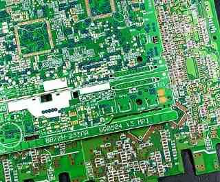
Figure 1.3 – Double-sided printed circuit board with silver-plated holes.
Typical parameters of double-sided boards:
Maximum workpiece dimensions - 300x250...500x500 mm;
The minimum hole diameter is 0.4...0.6 mm;
Minimum conductor width - 0.15 mm;
Minimum clearance - 0.15 mm;
Foil thickness - 18..36 microns;
Board thickness - 0.4 - 2.0 mm;
Based on the experience of many companies engaged in the production of printed circuit boards, prototypes from domestic customers of double-sided boards, it can be stated that the requests of domestic developers are so far satisfied by the range of design standards 0.2 / 0.2 - 0.3 / 0.3 mm, standard 0.15 / 0.15 mm occurs in no more than 10% of cases.
Note that domestic developers, just like their foreign colleagues, put technical specifications for the production of double-sided circuit boards solder mask, marking, quite often - milling boards along a complex contour. As a rule, the assembly of such boards involves surface mounting of components.
Multilayer printed circuit boards.
Multilayer printed circuit boards (MPBs) account for two-thirds of global printed circuit board production in terms of price, although in quantitative terms they are inferior to single- and double-sided boards.
The structure of MPP is much more complex than double-sided boards. They include additional shield layers (ground and power), as well as several signal layers. Figure 1.4 shows a block diagram of a multilayer printed circuit board.
To ensure switching between MPP layers, interlayer vias and microvias are used.
Interlayer transitions can be made in the form through holes connecting the outer layers to each other and to the inner layers, blind and hidden transitions are also used.
A blind via is a metallized connecting channel visible only from the top or bottom side of the board. Hidden vias are used to connect the internal layers of the board to each other. Their use makes it possible to significantly simplify the layout of boards; for example, a 12-layer MPP design can be reduced to an equivalent 8-layer one. switching

Figure 1.4 – Structure of a multilayer printed circuit board.
Microvias have been developed specifically for surface mounting, connecting contact pads and signal layers.
To manufacture MPPs, several dielectrics laminated with foil are connected to each other, for which adhesive gaskets - prepregs are used. Therefore, the thickness of the MPP grows disproportionately quickly with an increase in the number of signal layers.

Figure 1.6
In this regard, it is necessary to take into account the large ratio of the thickness of the board to the diameter of the through holes. For example, for an MPP with a hole diameter of 0.4 mm and a thickness of 4 mm, this ratio is 10:1, which is a very stringent parameter for the process of through-hole metallization.
However, even taking into account the difficulties with metallization of narrow through holes, MPP manufacturers prefer to achieve a high density of installation due to a larger number of relatively cheap layers rather than a smaller number of high-density but, accordingly, more expensive layers.
In modern MPPs, surface mounting of all types of modern integrated circuits is widely used, including, as shown in the figure, unpackaged circuits filled with compound after welding the leads.
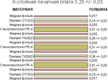
Figure 1.7 – An example of the thickness of an 8-layer printed circuit board.
Flexible printed circuit boards.
The use of flexible dielectric materials for the manufacture of printed circuit boards provides both the designer and user of electronic devices with a number of unique opportunities. This is, first of all, reducing the size and weight of the structure, increasing assembly efficiency, increasing electrical characteristics, heat transfer and overall reliability.
If we take into account the main property of such boards - dynamic flexibility - it becomes clear that the increasing volume of applications of such boards in automobiles, household appliances, medicine, defense and aerospace equipment, computers, industrial control systems and on-board systems becomes clear.
Flexible printed circuit boards (FPCs) are made on polyimide or Mylar film and therefore can easily deform even after forming a conductive pattern. Most of The designs of flexible PCBs are similar to the designs of printed circuit boards on a rigid base.
Unilateral GPP- are the most common in this class of boards, since they exhibit the best dynamic flexibility. The contact pads of such boards are located on one side; copper is most often used as the conductive foil material.

Single-sided gas pumps with two-way access have one conductive layer, the contact pads for which are made on both sides of the board.

Bilateral GLP have two conducting layers that can be connected through metallized vias (in the figure, the conductors of the lower layer run perpendicular to the conductors of the upper layer). This type of board provides high density installation, are often used in electronic devices with controlled impedance of the boards.

Multilayer GPP contain at least three conductive layers connected by metallized holes that provide interlayer connection. In such boards it is easier to implement high packing density, since it is not necessary to provide large values"height/hole diameter" ratios. It is predicted that such GPPs will be used for assembling multi-chip integrated circuits on them.

Rigid-flexible PP are hybrid structures and contain both rigid and flexible bases, fastened together into a single assembly and electrically connected by metallized holes. They are most common in defense equipment, but their use is also expanding in industrial electronics.

GPP with local tightening (strengthening).In such boards it is possible to place rigid metal parts inside a flexible base. Produced by a multi-step process of photolithography and etching.
![]()
Relief printed circuit boards (RPC).
The design and manufacturing technology of RPPs differ significantly from traditional double-sided (DPP) and multilayer (MLP) boards. Note that the authors of most designs and technologies of RPP in our country are A.V. Bogdanov and Yu.A. Bogdanov.
RPP (Figure 1.8) is a dielectric base into which copper conductors, made in the form of metallized grooves, and through metallized holes, having the shape of two converging cones. Such grooves and holes are filled with solder. Typically, RPPs have two conductive and one insulating layer.

Figure 1.8 – Relief printed circuit board.
As can be seen from Figure 1.9, the elements of the conductive pattern can be of the following types:
straight conductors on the first and second layers; metallized transition holes (for electrical connection pattern elements on conductive layers);
through mounting holes metallized (for mounting pin terminals of electronic components;
metallized lamellas (for mounting planar leads of electronic components;
blind mounting holes (for mounting planar leads of electronic components molded for butt soldering).
The conductors are straight and parallel to the X and Y axes, which is due to the peculiarity of the technological equipment for manufacturing the grooves.

Figure 1.9 – Drawing of conductive elements.
Characteristics of relief boards.
The diameter of the transition metallized holes on the surface of the dielectric base does not exceed the width of the conductor. In this case, there are no contact pads around the vias. This makes it possible to set transitions in a tracing step (in adjacent tracing discretes) without any restrictions. Typically, RPP routing is carried out in a strictly orthogonal system, which means running horizontal conductors on one conductive layer, and vertical conductors on the other. This provides greater tracing capabilities than other systems, but it also introduces big number transitions. However, for RPP, unlike any other, transitions increase, rather than decrease, the reliability of the board.

Figure 1.10 – Main dimensions of the RPP.
The main parameter of the RPP design, which determines its other parameters, is the minimum tracing step minH. The use of a variable tracing step is essential here. Initially, this was dictated by the technological equipment used, which provided movement with a resolution of 10 microns. Later it was discovered that this increases routing capabilities due to the symmetrical passage of traces through most mounting points. Additionally, variable pitch allows for improved manufacturability by moving the centers of vias away from the edges of the mounting points.
Figure 1.11 shows options for the used constant and variable routing steps for RPP with microcircuits having following types and external pin pitches: pin - 2.5 mm, planar - 1.25 mm and planar - 1.0 mm.

Figure 1.11 - Variants of used constant and variable tracing steps.
Table 1 shows typical values of the design parameters of the RPP for minH Fig. 3. And the table shows that a feature of the RPP is its small thickness compared to PP. This, combined with the metal saturation of the dielectric base, provides good thermal conductivity. The cross-section of copper in the grooves provides a linear resistance of 3-3.5 Ohm/m and a maximum current through the conductor of 300-400 mA. These parameters should be taken into account when designing power circuits, as well as high-current signal circuits.
Table 1 - Typical values of design parameters of the RPP.
A small routing step in combination with vias in the routing step provides high routing capabilities of the RPP.
Comparison of technological and cost characteristics of relief and multilayer printed circuit boards:
Traceability
The density of placement of elements on the RPP is equivalent to 6-8 layers of MPP. For example, up to 5 conductors can be routed between the pins of a standard DIP package. The high routing ability is explained, in particular, by the fact that vias can be located in the conductor pitch.
Electrical characteristics
Since the cross-section of the RPP conductor has the shape of a trapezoid, its direct current resistance is 1.5 times less than that of flat conductors. Characteristics according to alternating current RPP and MPP do not differ significantly.
Mechanical characteristics
RPP is a fundamentally thin board (0.8 mm). Therefore, to install massive elements or large boards, mechanical reinforcement is required. But, on the other hand, RPP is very resistant to bending. For RPP, deflections of up to 40-50% are not scary.
Manufacturing of lamellas
RPP are thin boards, so direct production of lamellas for ISA-RS type connectors may not provide sufficiently reliable contact. To solve this problem, there is a special technological technique that makes it possible to obtain double the thickness (1.5 mm) in the area of the lamellas, which ensures a reliable connection.
Resistance to external factors
RPP is in no way inferior in resistance to impact external factors traditional boards. Moreover, the metallization of RPP is made of chemically homogeneous copper and for RPP the problem of contact in the area via absent.
CAD support
The RPP manufacturing system is compatible with almost any CAD system: PCAD 4.5 .. 8.5, etc.
Serialization
The production of RPP does not imply any special preparation for production (photo templates, matrices). The production time for a medium-complexity board is 48 hours. The cost of RPP is noticeably lower than the cost of multilayer boards for small series of up to 100 - 1000 pcs. However, as the quantity increases, the cost does not decrease as significantly as for multilayer or double-sided boards. Therefore, the production of RPP batches of more than 10,000 must be carefully economically justified.
Cost characteristics
When comparing eight-layer MPP with RP according to average cost indicators, a decrease is obtained:
for milling methods - approximately 16 times;
for the pressing method - approximately 36 times;
for the casting method - approximately 100 times.
High density printed circuit boards.
An example of a high-density printed circuit board is shown in Figure 1.13

Assembly and installation of elements on printed circuit boards.
A feature of modern electronic device production is the increasingly widespread use of large and ultra-large integrated circuits (LSI and VLSI). At the same time, the number of pins of each circuit increases significantly, the distances between the pins are reduced from 2.5 mm to 0.625 mm or less.
Installing multi-pin LSI and VLSI packages on printed circuit boards is technically and economically more efficient not in through holes, but on contact pads located on the surface of printed circuit boards.
This explains the increasingly widespread transition from mounting components in holes (PTH - Plated Through Hole) to surface mounting technology (SMT - Surface Mount Technology).
At the same time, at present, most serial electronic units use both surface mounting and through-hole mounting. This is due to the fact that the designs of some components are not suitable for surface mounting. In addition, in devices operating under conditions of shock and vibration overloads, hole mounting is preferred due to more reliable fastening of components.
The process of installing elements on the RP does not differ significantly from standard processes. Installation in holes and on the surface is possible using hand soldering, wave soldering, soldering in infrared and convection ovens. The only thing that needs to be taken into account when molding and installing the elements is that the mounting lamellas are recessed by 0.1 mm relative to the surface of the board.
TypesSMTassemblies.
Surface-Mount Technology (SMT) - surface mounting technology.
In the electronics industry there are six common types SMT assemblies, each of which has its own production order. When a designer selects an assembly type, the goal should be to minimize the number of operations, since each operation can add industrial cost. There is a special standard that presents the main types of assemblies, divided into classes.
SMC and IPC documentation for surface mount boards, IPC-7070, J-STD-013 and the National Technology Roadmap for Electronic Interconnections include the following classifications of the following surface mount circuits:
Type 1 - mounted components installed only on the top side or interconnecting structure
Type 2 - mounted components installed on both sides of the board or interconnecting structure
Class A - through-hole components only
Class B - surface mount components (SMD) only
Class C - mixed: through-hole and surface mount components
Class X - complex mixed assembly: through-hole, SMD, fine pitch, BGA
Class Y - complex mixed assembly: through-hole, surface mount, Ultra fine pitch, CSP
Class Z - complex mixed assembly: through-hole, Ultra fine pitch, COB, Flip Chip, TCP
Operations are used for various types of assembly:
Paste application and installation SMT components on the top side of the board.
Applying paste and installing SMT on the bottom side of the board.
Applying glue and installing SMT components on the underside of the board and then allowing it to dry.
Automatic installation of DIP components.
Automatic installation of coordinate components (such as LEDs, etc.).
Manual installation of other components.
Wave soldering or infrared soldering.
Washing boards.
Hand soldering of components.
Below we will discuss the main options for placing components on the board used by developers. Options that use packages of components such as: Ultra fine pitch, COB, Flip Chip, TCP are not yet being considered, since they are almost never used by Russian printed circuit board developers.
Type 1B: SMT Top side only
This type is not common since most designs require some DIP components. It is called IPC Type 1B.
The order of the process: applying solder paste, installing components, soldering, washing.
Type 2B: SMT Top and Bottom Sides
On bottom side The boards house chip resistors and other small components. When using wave soldering, they will be re-melted by the overhead (side) flow of the solder wave. Placing large components on both sides, such as PLCC, increases production costs because the components on the bottom side must be mounted with a special conductive adhesive. This type is called IPC Type 2B.
Procedure for carrying out the process:
applying solder paste, installing components, soldering, washing the underside;
Applying solder paste to the top side of the PCB, installing components, re-soldering, washing the top side.
 (1 ratings, on average: 5,00 out of 5)