Monitor power supply and inverter. Typically, the control node, PWM and brightness control node are combined in one chip. The converter is made on discrete elements with a load in the form of a pulse transformer, the additional winding of which is used
Hi all!
In this article we will explain to you what it is , what significance does it have in lcd panels and how it works.
An inverter is a converter of direct voltage (usually 12V) into high-voltage alternating voltage.
In order for the LCD panel to provide a bright image, a light flux is needed, which is passed through the matrix and, in fact, forms the image on the screen. In LCD monitors to create such luminous flux fluorescent lamps are used lamps backlight cold cathode (CCFL). In monitors, these lamps are usually located along the edges (top and bottom), and in TVs, directly under the matrix throughout the entire area. Using filters and a diffuser, the lamps evenly illuminate the entire surface of the matrix. In order to ensure the starting or “ignition” of lamps with a voltage of more than 1500V, and then powering these lamps for a long time in operating mode with a voltage of 600...1000V, inverters are used.
In LCD monitors, lamps are connected using a capacitive circuit.
The inverter provides the following functions:
converts direct voltage into high-voltage alternating voltage;
stabilizes and regulates the lamp current;
provides brightness adjustment;
ensures coordinated operation of the inverter output stage with the input resistance of the lamp;
creates protection against overloads and short circuits.
Structural

As shown in the diagram, the standby mode unit, as well as the inverter switching on, is made on keys Q1 and Q2. Since the monitor takes a little time to turn on, the inverter turns on 2...4 seconds after the monitor is switched to operating mode. When voltage is ON. (on/off), the inverter enters operating mode. This unit also turns off the inverter if the monitor goes into saving mode.
When the switch base Q1 receives positive voltage ON. (3…5V), +12V voltage is supplied to the brightness control unit and the PWM regulator.
The unit for monitoring and controlling the brightness of lamps and PWM (3) is made according to the circuit of an error amplifier (EA) and a PWM pulse shaper. This node receives the dimmer voltage from the main monitor board, then this voltage is compared with the voltage feedback, and then an error signal is generated that controls the frequency of the PWM pulses. These pulses control the DC/DC converter (1) and synchronize the operation of the converter-inverter. The amplitude of the pulses is constant and is determined by the supply voltage (+12V), and the frequency of the pulses depends on the brightness voltage and the threshold voltage level.
Thanks to the DC/DC converter, a constant (high) voltage is supplied to the autogenerator, which is turned on and controlled by PWM pulses of the control unit (3).
output level AC voltage The inverter depends on the parameters of the circuit components, and its frequency is determined by the brightness control and the characteristics of the backlight lamps. The inverter converter is usually a self-excited generator. Schemes can be used both single-cycle and two-cycle.
The protection unit (5 and 6) analyzes the level of current or voltage at the inverter output and generates feedback and overload voltages, which are supplied to the control unit (2) and PWM (3). If the value of one of these voltages exceeds the threshold value (short circuit, converter overload, undervoltage), the oscillator stops operating.
Typically, the control node, PWM and brightness control node are combined in one chip. The converter is made on discrete elements with a load in the form pulse transformer, the additional winding of which is used to switch the triggering voltage.
All main inverter components are housed in SMD component housings.
There are a huge number of modifications of inverters.
Backlight power supplies and inverters are something that is of increasing interest to LCD monitor repair specialists. And this is understandable, because these modules give the highest percentage of failures. The circuitry of these modules is not too complicated - experienced specialist He can easily figure it out without a schematic diagram, and even more so if he has a description of the elemental base. Nevertheless, circuit diagram on the repaired node has never interfered with anyone. Thus, the power supply and inverter diagram is the most valuable part of the service manuals. But many manufacturers, and among them Samsung, rarely provide this most needed information in their manuals for diagnosing and repairing monitors, which greatly complicates the life of unauthorized services. We hope that the result of studying the Samsung SyncMaster 943N monitor inverter presented here will help you in your work.
Like most modern monitors, the Samsung SyncMaster 943N adopts the concept that the monitor has two printed circuit boards: Scaler/microprocessor board and combined power supply board, which houses the monitor power supply (Power Supply) and backlight inverter (Back Light Inverter).
In this review we are looking at such a well-known combined inverter and power supply board for monitors of the SyncMaster 943N family,
Although monitors of this model can be equipped with other types of combined board. The PWI1904SJ board (also called McKinley 17"/19" Normal) has undergone several modifications (revisions). We will consider the board version 1.1 (Rev.1.1). It should be noted that the Samsung catalog number for this board is BN44-00123L.
So, as already mentioned, the board consists of two, almost independent, parts. Let's give brief description each of them.
Power supply
The power supply provides the formation of two output voltages direct current: +15V and +5V. The power source is a classic single-ended pulse flyback converter. The main element of this source is a PWM controller with a built-in power switch - the DM0456R microcircuit. It is this microcircuit that determines the circuit design of the entire source, which, by the way, is very simple (if you don’t use the word primitive).
Backlight Inverter
The inverter provides the formation of a high-frequency alternating voltage of 650V on four backlight lamps. The lamp current is at 7.5 mA. The inverter uses a fairly advanced version of circuit technology - a resonant converter. The inverter supports all basic protection options (overvoltage protection, lamp breakage protection), the inverter is controlled by the FAN7314 controller (see previous article). +15V is used as the inverter supply voltage.
Schematic diagram of the board
Power supply
The power supply, being a switching one, consists of a standard set of nodes, each of which performs a corresponding function. We will not give a detailed description of each node, because, as mentioned above, the power supply is built according to a classical scheme, and we do not set the goal of this review to study the basics of pulse converters. Let us focus on comparing the main components of the power supply and electronic elements of the presented circuit.
Input circuits
The input connector to which AC mains voltage is supplied is connector IN101. Protection against excess input current is provided by fuse F101 (3.15 Amperes).
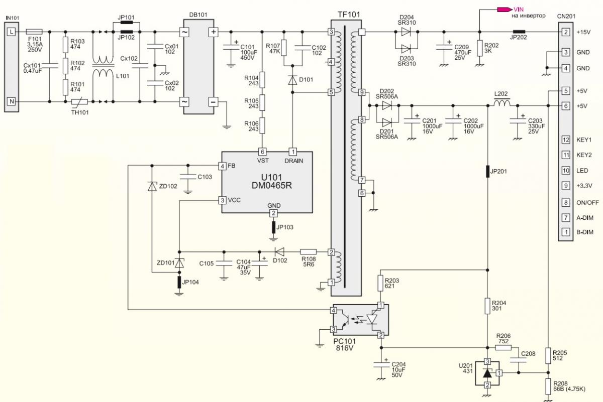

Input network filter formed by the following elements: capacitors Cx101, Cx102, Cx01, Cx02, resistors R101, R102, R103, inductor L101, thermistor TH101.
Mains voltage rectification is provided by the DB101 integrated diode bridge, and smoothing electrolytic capacitor C101.
Pulse converter
The main element of the converter is a PWM controller with a built-in power switch - an integrated 5-pin microcircuit on the radiator, with the position designation U101. This scheme uses a very popular Lately microcircuit - DM0465R. We will not discuss this controller, since finding its description is not difficult.
The starting circuit of the DM0465R PWM controller is formed by resistors R104, R106, R106 with a resistance of 24 kOhm each.
The power supply circuit of the DM0465R PWM controller in steady state is formed by resistor R108, diode D102, and capacitors C104 and C105. The energy source for powering the PWM controller in operating mode is the winding of the pulse transformer TF101 (pin 1-pin 2). The supply voltage is limited by the Zener diode ZD101.
The snubber, which provides suppression of resonant voltage surges in the primary winding of the pulse transformer TF101 when switching the power transistor, consists of diode D101, resistor R107 and capacitor C102.
The feedback signal, which allows you to stabilize the output voltages of the power supply, is supplied to pin 4 of the DM0465R PWM controller. The magnitude of the feedback signal on pin 4 is controlled by the optocoupler RS101.
Secondary rectifiers
Secondary rectifiers are made according to a half-wave circuit.
The rectifying diodes of each channel consist of a pair of diodes connected in parallel. This allows you to increase the current load of the channels.
Smoothing of rectified pulses in the +15V channel is ensured by capacitor C209 and capacitors C206, C207, C31, which we assigned to the inverter circuit.
Smoothing of pulses in the +5V channel is provided by capacitors C201, C202, C203, as well as inductor L202.
The feedback signal to ensure stabilization of the output voltages is generated from the +5V channel voltage using a divider R205/R20S. The voltage obtained by this divider controls the U201 microcircuit of the TL431 type (controlled regulator). This microcircuit, in turn, controls the current through the LED of the RS101 optocoupler, which ultimately changes the value of the feedback signal on pin 4 of the DM0465R PWM controller.
Backlight Inverter
The load of the backlight inverter is four, connected to four connectors: CN1, CN2, CN3, CN4. The high-voltage transformer is T1 with two primary and two secondary step-up windings.
The inverter is made according to a resonant circuit. The resonant circuit is formed primary windings transformer T1 and two parallel SMD capacitors: C32 and SZZ. Thus, the resonant circuit is series.
The inverter supply voltage is +15V, which is supplied to the inverter through fuse F201 (3 Amperes). This voltage is used both to power the control microcircuit and to power the power stage - the resonant circuit.
Oscillations in the resonant cascade are ensured by synchronous switching of two power transistors in an integrated design (type transistor assembly). The transistors are field-effect ones: one of them is P-channel (upper key), and the other is N-channel (lower key). The transistors are controlled by the FAN7314 backlight controller.
Since the controller is designed to control a bridge converter, and this circuit uses only two transistors, not four, the two outputs (OUTC and OUTD) of the microcircuit are not used (pin 14 and pin 15). Antiphase pulses are formed at the OUTA and OUTB pins (pin 18 and pin 19). The pulses follow with a frequency of several tens of kHz (but the sequence of pulses is interrupted, forming so-called “packs” - see below about brightness adjustment). This frequency is set by capacitors C5, C24, C25. Depending on the modification of the board, capacitors C24 and C25 may be included in different combinations. Jumpers are provided for these purposes. In addition, the frequency of the internal generator is also set by the value of resistor R5.
Current feedback To stabilize the lamp current, i.e. To stabilize their brightness, inverters use negative current feedback. To provide current feedback, a current sensor - a resistor with a resistance from several hundred Ohms to 1 kOhm - is connected in series with the lamps. These resistors are traditionally precision (with a tolerance of 1% tolerance). A voltage is removed from the feedback resistor, the magnitude of which is directly proportional to the magnitude of the current flowing through the lamps, and therefore proportional to the brightness of the lamp.
In the presented circuit, such current sensors are R16, R17, R18, R19, rated at 1 kOhm. The signals taken from all four sensors are combined into one point, where the resulting feedback voltage is formed. The summation of current sensor signals is carried out using decoupling diodes of diode assemblies D6, D7, D8, D9. The resulting feedback voltage is supplied to pin 9 of the FAN7314 controller through a chain of matching resistors R15, R9, R8.
The A-DIM signal is also added to the feedback signal, which is an analog brightness control signal. The A-DIM signal is generated by the monitor's microprocessor and changes its value when the brightness is adjusted by the user. The signal is a DC voltage, increasing the A-DIM signal leads to an increase in the feedback voltage, and, as a result, to a decrease in the lamp current. And vice versa.
Overvoltage protection
Protection against overvoltage on lamps is provided by a voltage feedback signal. A capacitive voltage divider is connected to the “hot” contact of each lamp connector (C8/C29, C7/C15, C9/C30, C10/C14). At the midpoint of each divider, an alternating sinusoidal voltage is generated, proportional to the voltage across the lamps. Next, all four voltages are rectified and summed using diodes, diode assemblies D3 and D4. The resulting voltage is applied to pin 2 (OLR) of the FAN7314 controller. Smoothing of the summing voltage is provided by capacitor C16. Diodes D3 and D4 set the OLR pin to a voltage that is the highest of the four voltage feedback signals. In other words, excess voltage on any of the four lamps triggers this protection.
Lamp break protection
An open lamp circuit is the most dangerous situation for the inverter. This causes failure power keys inverter, because the inverter, which is a pulse converter, starts to idle without load. Breakage of the lamps in this circuit, as well as in most others, is determined by the absence of voltage on the lamp current sensor resistors (R16 ... R19).
When current flows through the lamps, a voltage is formed on resistors R16 ... R19, which is smoothed out by capacitors C17, C16, C19, C20. As a result, a voltage is set on these capacitors, which ensures that the diodes of the diode assemblies D10 and D11 are blocked. Closed state all these four diodes ensure the open state of transistor Q1, because the base of this transistor is biased by the value of the reference voltage VREF generated by the FAN7314 controller.
If at least one lamp breaks, then one of the four diodes of the D10 and D11 assemblies immediately opens, because On the cathode side of the corresponding diode, the blocking voltage disappears. This, in turn, leads to the closing of transistor Q1 and blocking the FAN7314 controller.
Brightness control
The inverter under consideration uses the Burst Dimming brightness adjustment method (intermittent adjustment method), which assumes that the lamp current represents “packs” of high-frequency alternating current(Fig. 2). A “pack” corresponds to the on state of the lamp, and between packs, accordingly, the lamp turns off. The width of these packs, i.e. The ratio between the on and off states of the lamps determines the brightness of the backlight. As the brightness increases, the width of the “packs” increases, and at the maximum brightness level, the current in the lamps becomes virtually continuous.

Brightness adjustment in this circuit is carried out by two signals: A-DIM and B-DIM, generated by the monitor’s microprocessor.
The B-DIM signal is supplied to the inverter input via pin 1 of the CN201 connector. The B-DIM signal is a low-frequency pulse that follows at a frequency of approximately 200 Hz. When adjusting the brightness, the width of these pulses changes. It is the width of these pulses that determines the width of the “packs” of alternating current in the lamps.
The A-DIM signal is supplied to the inverter input via pin 7 of the CN201 connector, and represents a DC voltage. This signal is mixed with the feedback signal supplied to pin 9 of the FAN7314 chip. When adjusting the brightness, the A-DIM signal practically does not change. A significant jump in the A-DIM signal level occurs when changing color palette through the Magic Bright menu, and only when selecting certain settings in this menu.
Inverter faults
Inverters of the PWI1904SJ(M) family are characterized by two faults:
- failure of the transistor assembly;
- failure of transformer T1.
Failures of other elements of the circuit are extremely unlikely, so it makes no sense to talk about them, but it is necessary to discuss the most probable failures.
Transistor assembly The STU407DH assembly is a pair of field-effect transistors of different conductivity: N-channel and P-channel. Internal assembly architecture and its appearance are presented in Fig. 3.
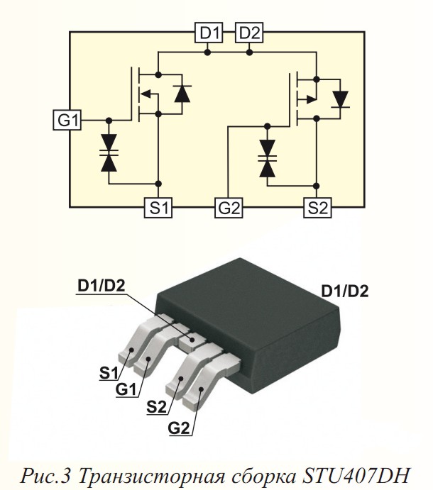
Main electrical characteristics The transistors in the assembly are as follows:
- drain-source voltage: 40V;
- gate-source voltage: 20V;
- Drain current (for P-channel): -12A;
- Drain current (for N-channel): 16A;
- Pulse drain current: 50A;
- forward current of the damper diode (for P-channel transistor): -6A;
- forward current of the damper diode (for N-channel transistor): 8A;
An assembly malfunction consists of a breakdown of one or two transistors in the assembly. Diagnostics of the assembly, naturally, is carried out with a tester (ohmmeter), and consists of alternately checking two field-effect transistors (we will not go into how to test field-effect transistors here). It should also be noted that analogs of this transistor assembly are not known, so if the STU407DH fails, you will have to purchase it.
Transformer
The type of transformer used in this inverter is .
Typical fault of this transformer is a break (or “burning”, i.e. an increase active resistance) one of the two secondary high-voltage windings.
The parameters of these secondary windings of a working transformer are as follows:
- active resistance: 1120...1130 Ohm;
- inductance: 1.93...1.95 H.
Based on the data presented. We can say that diagnosing a transformer is a very mediocre matter, feasible with the help of the simplest tester. It is enough just to measure the resistance of the secondary high-voltage windings. But I would like to note that the value of the winding resistance may be different, so when checking a transformer, it is better to compare the resistance of its two high-voltage windings. If the resistances are the same, then the transformer is working. And if the resistances differ by 100 Ohms or more, then we can talk about a malfunction of the transformer, and the faulty winding should be considered the one with the highest resistance.
What to do if one of the windings is broken, or its resistance has increased?
First solution. The most simple solution is to replace the transformer. Acquiring it at the moment should not be difficult. “Compatible” transformers with similar characteristics are widely available on the market. However, it should be borne in mind that when purchasing a “compatible” transformer, it is quite possible to encounter a situation where, with a replaced transformer, the inverter does not work at all, or after a while the protection is triggered.
Second solution. Another solution to the problem of a faulty transformer is to convert the inverter circuit to work with two lamps.

To do this you will have to do the following:
- remove the faulty high-voltage winding;
- block protection against lamp breakage;
- remove resistor R31.
The faulty winding will have to be completely removed (Fig. 4). Disconnecting the load from the faulty winding (i.e. two lamps) does not give any result, and when operating at idle speed (with the protection blocked), the transformer heats up very much. Protection against lamp breakage, as mentioned earlier, is organized through two diode assemblies: D10 and D11. Therefore, blocking the protection involves unsoldering one diode assembly corresponding to the “arm” of the inverter in which the high-voltage winding was removed. Next, to reliably start the inverter, we remove resistor R31 from the circuit.
After this, the circuit can be started, and two lamps need to be connected to the remaining winding. To ensure uniform illumination of the screen, it is advisable to make sure that one upper lamp and one lower one are connected to the remaining winding. The length of the connecting wires of the lamps in monitors with the PWI1904SJ(M) inverter allows such switching to be done without problems.
This article discusses the main points that need to be taken into account when repairing inverters for LCD TVs and monitors.
LCD TV inverter repair.
If you want to repair such a device yourself, then you need to understand that you will need some knowledge and skills. If there is no experience, then it is better to call the master.
Television inverter is a device that is responsible for starting and uninterrupted operation of the backlight of any LCD panel. You can also use it to easily increase or decrease the brightness of an image. Before proceeding with the elimination possible malfunction this device, you need to understand what it does:
First of all, the device converts the voltage, which usually does not exceed 24 V, into high voltage.
The second responsibility is to regulate the supply in fluorescent lamps, as well as its stabilization.
As mentioned above, changing the brightness is also his direct responsibility.
One of the most useful functions is to protect the TV from all kinds of overloads, as well as to prevent short circuits.
Faults directly related to the inverter:
The backlights do not turn on or work intermittently.
Spontaneous changes in screen brightness or flickering.
When the inverter refuses to work after a long period of inactivity, this is one of the most serious malfunctions.
Unequal backlighting of the screen in the presence of a circuit of 2 devices also refers to problems.
Troubleshooting:
If one of the above malfunctions is detected, then you first need to check the voltage for absence of ripple and stability.
Then you need to pay attention to the quality of the commands associated with turning on the lamps and adjusting the backlight. They come from the motherboard.
If the problem is still not found, you need to remove the protection from the inverter itself and start looking for a breakdown. Next, a careful inspection of the board for burnt elements follows.
After this, it doesn’t hurt to measure indicators such as voltage and resistance using a tester.
It is also worth paying attention to checking transistor switches; they are often to blame.
Then comes the inspection of high-voltage transformers. Improper assembly or poor insulation of these devices can also cause problems. On transformers, breaks and short circuits of individual turns can still occur. Such problems are also identified during inspection and testing of the device.
LCD monitor inverter repair.
Most computer monitors inevitably develop problems over time. And in most cases they are all exactly the same.
Monitor problems :
Screen backlight failure due to non-functioning lamps.
Turning on the lamps for a short period of time and then turning them off.
Unstable monitor brightness, flickering.
Troubleshooting
The first thing you need to do is check the voltage in the power system, the normal value is more than 12 V. If it is not there at all, then you need to check the fuses. If the problem is here, then before making a replacement, you need to inspect the transistors.
If the above operations are useless, the microcircuit must be completely changed. Now you need to inspect the converter for generation failure. Checking the transistors will also not be superfluous.
Next, the ENB signal should be checked. If it is not there, then the problem must be looked for in the main board. If there is a signal, then you need to inspect all the lamps and look for damage or burnt elements. If the problem still persists, then the secondary circuits should be checked next, so the protection that protects against short circuits may work. For the same purpose, you can inspect the transistor, divider, and zener diode. In a situation where the voltage at the terminals is less than 1 V, a new capacitor must be installed.
Then follows a study of the stability of the brightness voltage of the resistor, which must be disconnected from the feedback before testing. If the voltage is not stable, then the problem lies in the main board of the monitor. The next step is to check the oscillations and stability of the so-called sawtooth pulse generator. The amplitude should be in the range from 0.7 to 1.3 V. The frequency indicator should be around 300 kHz. If the voltage is unstable, then the device needs to be changed.
 (1 ratings, on average: 5,00 out of 5)